MCU–FPGA Development Board Bring-Up and Digital I/O Validation
Introduction
In this lab, we soldered our E155 protoboard and implemented designs on the FPGA to drive on-board LEDs and a seven segment display. Two of the LEDs outputted combinational logic, and one of them was blinked at a specific frequency using the on-board high-speed oscillator.
Design and Testing
After soldering and testing the FPGA, MCU, and the development board for proper functionality, I designed my FPGA to further test the hardware on my board and operate a 7-segment display. The design consisted of the following:
| Signal Name | Signal Type | Description |
|---|---|---|
| clk | input | 48 MHz clock on FPGA |
| s[3:0] | input | four DIP switches (on the board) |
| led[2:0] | output | 3 on-board LEDs |
| seg[6:0] | output | the segments of a common-anode 7-segment display |
There were two primary aspects to this lab: operate three on-board LEDs (led[0], led[1], and led[2]) and create a 7-segment display.
The relationship between the switches (s0, s1, s2, s3) and the first two LEDs (led[0] and led[1]) were provided in the form of truth tables. Upon deriving the combinational logic, it was clear that led[0] was an exclusive or (XOR) of s0 and s1, while led[1] was an AND of s2 and s3. The third LED, led[3], was to be blinked at 2.4Hz. This was done using the on-board high-speed oscillator (HSOSC) from the iCE40 UltraPlus primitive library. This oscillator generated a 48 MHz clock, and a counter was used to divide this down so the blinking frequency could be visualized on led[2]. In order to generate a 2.4 Hz signal that would complete a half cycle, a clock divider module was designed to count every (0.5)* 48 MHz/2.4 Hz, or 10 million ticks.
The 7-segment display was designed to display a signle hexadecimal digit specified by a four bit binary input s[3:0]. To do this, a separate SystemVerliog module was written, which contained 16 case statements detailing which segments of the display should be lit to create the hexademical digit corresponding to the dip switch input of s[3:0]. When breadboarding this design, it was important to remember that in the common annode display we were working with, a logic 0 applied to the cathode turned on the segment.
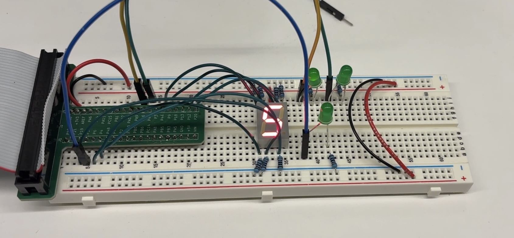
After designing the modules on SystemVerilog and programming the designs to the FPGA, we tested our design. For the LEDs, in order to test led[0] and led[1], we tried the different combination logic using the switches to ensure the proper XOR and AND gate functionality. For led[2], we used an oscilloscope to verify the blink frequency of 2.4 Hz. To test the 7-segment display, we operated the DIP switches to ensure that the four bit binary numbers displayed their corresponding hexadecimal digit with equal brightness in segments, as shown in Figure 1.
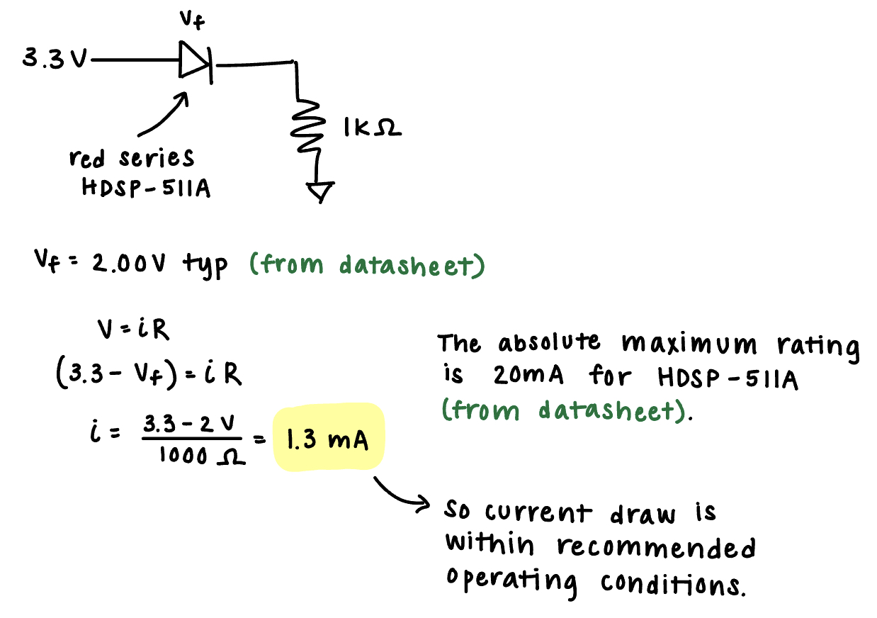
In order to enxure that the current draw for each segment in the 7-segment display was within recommended operating conditions, the calculations shown in Figure 2 were done. The absolute maximum current rating is 20 mA, and as the calculations show, we have a 1.3 mA current draw, which is standard for LEDs.
Technical Documentation
The source code for the project can be found in the associated Github repository.
Block Diagram
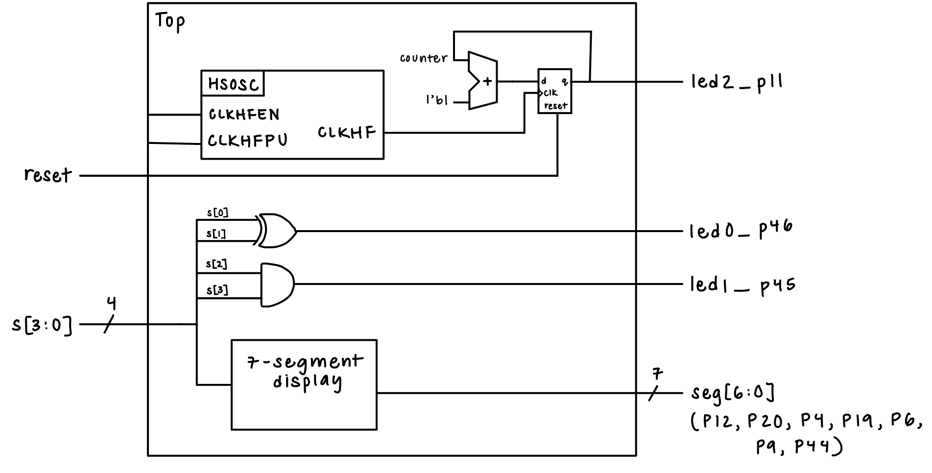
The block diagram shown in Figure 3 demonstrates the overall architecture of the design. The top-level module (top) includes two submodules: the high-speed oscillator block (HSOSC) and the module to operate the 7-segment display. The operation of the LEDs happens in the top-level module as combinational logic.
Schematic
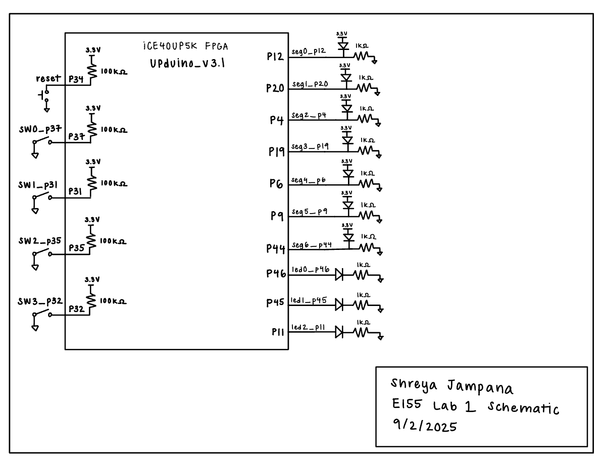
The physical layout of the design is shown in Figure 4. The left side of the UPduino shows the inputs, while the right side shows the outputs. The inputs consist of a reset button and four switches. An internal 100 kΩ pullup resistor was used to ensure the active low reset pin was not floating. The outputs consist of the seven LEDs from the 7-segment display, and three LEDs to test the combinational logic and blinking. These LEDs are connected using a 1kΩ current-limiting resistor to ensure the output current did not exceed the maximum output current of the FPGA I/O pins.
Results and Discussion
Testbench Simulation
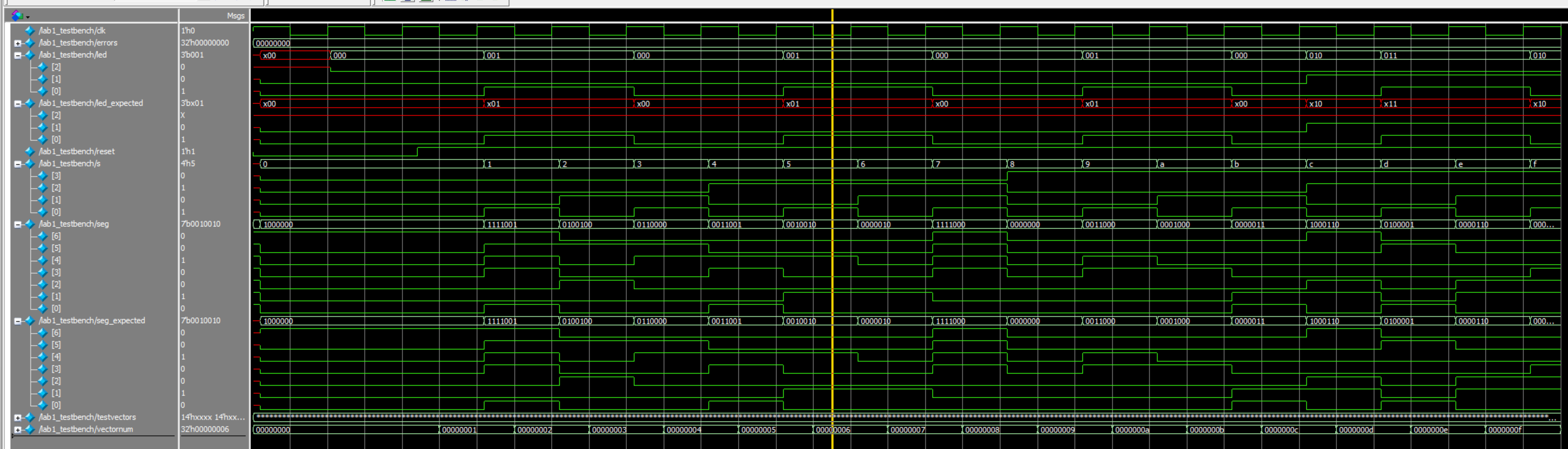
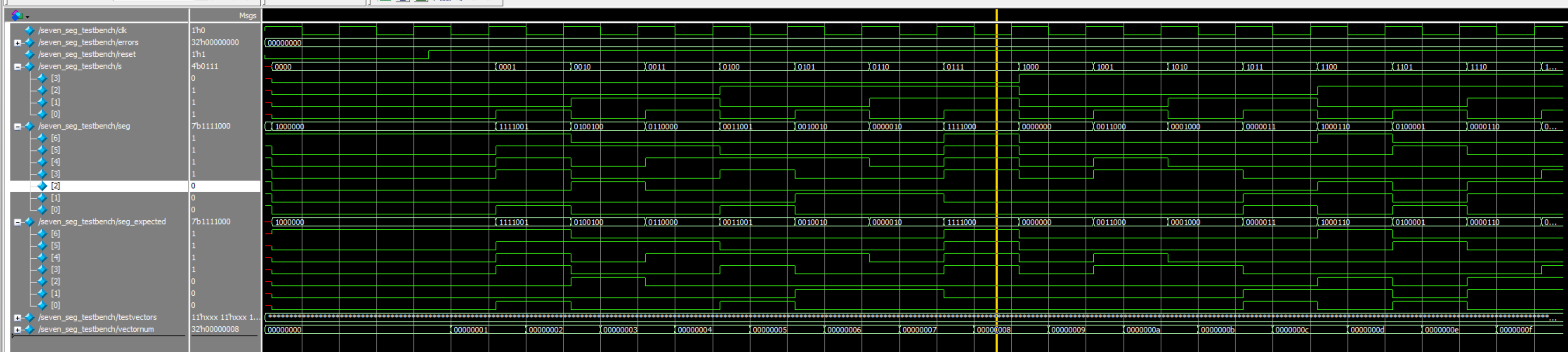
Two testbenches were written in SystemVerilog, one for the top-level and one for the 7-segment display modules, in order to verify that the designs were working as intended. Using the written test vectors, the testbenches ran all 16 cominations of the DIP switches in order to simulate and test if the led[2:0] and seg[6:0] outputs matched the expected outputs.
As shown in the simulation images shown in Figures 5 and 6, all the simulations passed and produced the expected outputs. Therefore, the design met all of the intended design objectives, and performed quickly and reliably. The simulations shown below ran in just a few seconds, and the hardware displayed all the required lights brightly.
Conclusion
My FPGA designs successfully controlled a 7-segment display and LEDs, thus validating the functionality of my soldered protoboard. By blinking one of the LEDs at 2.4 Hz, I also validated the functionality of the on-board high-speed oscillator.